Documentation
System Block Diagram:

FPGA Design
To implement the FFT in hardware on the FPGA, the team started by understanding the DFT algorithm in depth and consulting the paper titled by Alec and published by the HMC Dept. of Engineering.
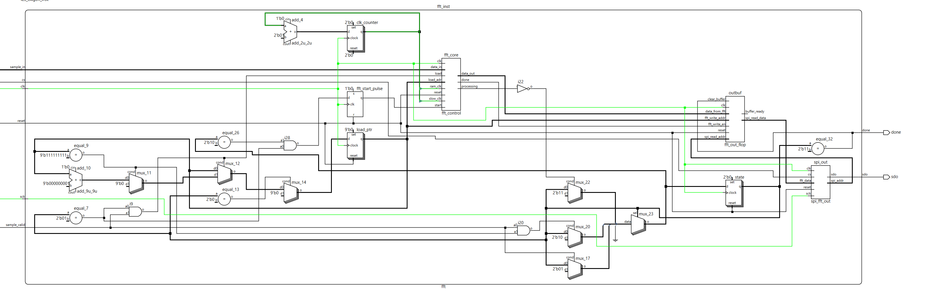
Each component of the FFT was designed in Lattice Radiant and adapted to be 512-point 32-bit resolution as shown in Figure 2 below. After building each component starting from the butterfly unit up to the FFT master module, each script was verified for accuracy against testbenches. Simulations involved testing cosine, square, and static input signals, ensuring that each transformed output was correct. To interface with the MCU, the SPI communication protocol was initialized at the end of the FFT data pipeline. The FPGA output on the SDO line was sent serially to the MCU.
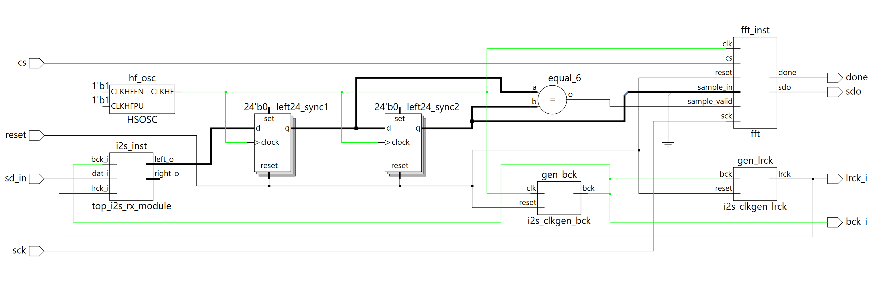
After the FFT was validated, the I2S module from the Lattice Radiant IP Block Catalogue was implemented. Since the INMP441 I2S microphone with a built-in ADC outputs 24-bit data but our FFT was configured for 32-bit resolution, sampled data was zero padded in the lower bits to achieve the required signal bit width. Additionally, the FPGA system clock of 48MHz from the instantiated HSOSC module was divided down to 3MHz for bck and 48kHz lrck output signals that were sent to the INMP441 to operationalize it. Figure 3 below shows the top level FPGA module that contains the I2S module and minimizes LUT and I/O pins.
New Hardware:
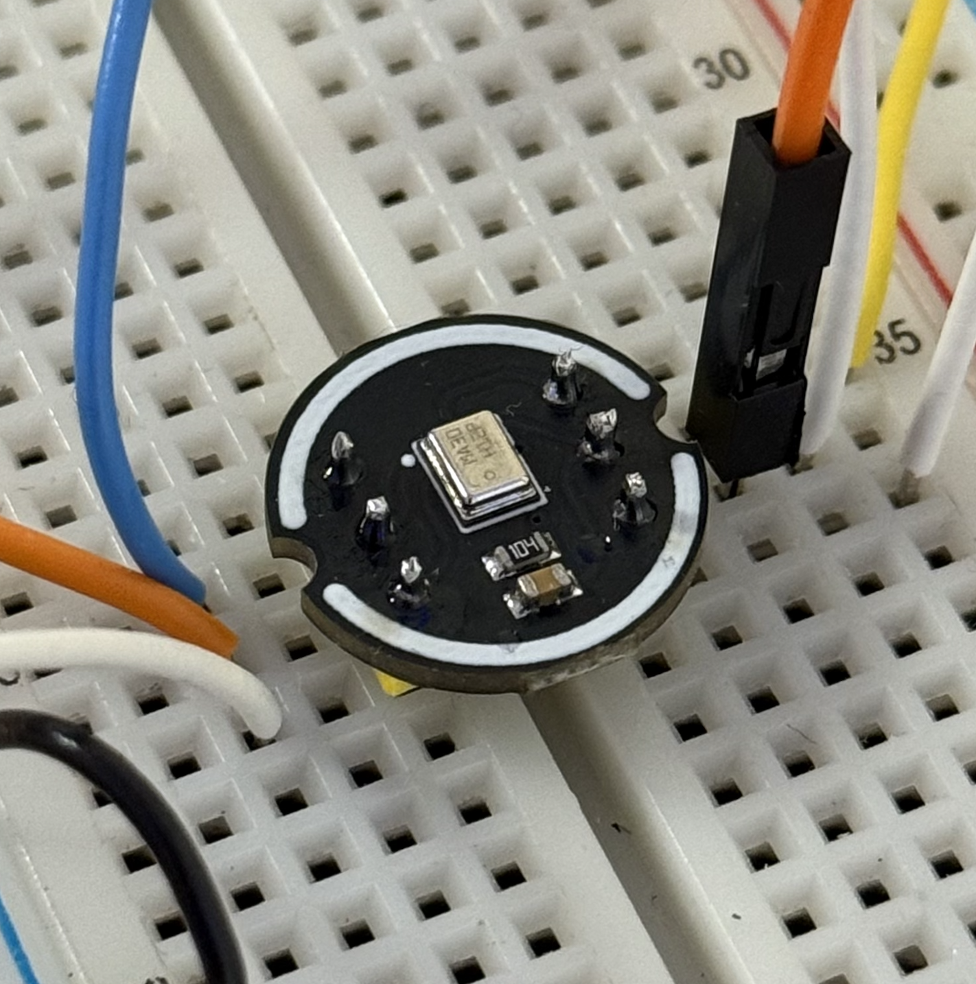
The primary new hardware component introduced in this project was the INMP441 digital I2S microphone shown in Figure 4 below, which represented a significant step beyond the SPI- and USART-based digital interfaces used previously in E155. Unlike these general-purpose serial protocols, I2S is specifically built for continuous, real-time audio collection, enforcing strict timing relationships between its bit clock (BCLK), left/right frame clock (LRCLK or WS), and serial data (SD) lines. These timing constraints required additional RTL modules and careful clock generation within the FPGA to ensure reliable audio sampling.
MCU Design
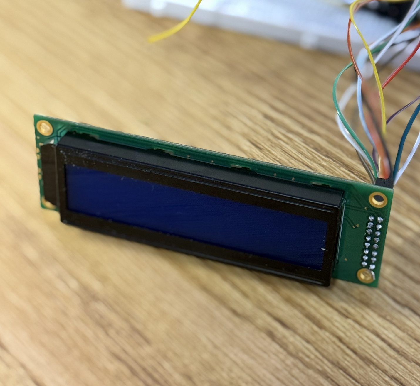
For this project, the MCU served as the control and interpretation layer for an FPGA-based 512-point FFT. The FPGA performs all real-time audio sampling and FFT computation, then signals the MCU through a DONE pin when a complete frame is ready. The MCU, acting as an SPI master, asserts chip-select, cs and clocks in all 512 complex FFT bins over an 8-bit receive-only SPI link, ignoring MOSI while using MISO to collect the FPGA’s streamed FFT output. Once a frame is received, the MCU computes the magnitude of each bin, identifies the dominant frequency using the 16 kHz sampling rate and 31.25 Hz bin resolution, and converts that frequency into a musical note using a flat-only chromatic scale (A, Bb, B, C, Db, etc.) along with a logarithmic cents-deviation calculation. These results— note name, pitch in Hz, and pitch deviation in cents—are displayed on a 16×2 LCD driven in 4-bit mode using dedicated GPIO lines. After updating the display, the MCU pulses a RST line to instruct the FPGA to begin processing the next audio frame. This architecture cleanly separates the heavy DSP work to the FPGA while the MCU handles control, interpretation, and user feedback.
New Hardware:
The new hardware interfaced with the MCU was the CFAH2002A-TMI-JT LCD screen shown in Figure 5 below. While in E155 simple 7-segment displays were explored in depth on the FPGA, LCD screens are far more complex in they are driven as well as their capabilities to control backlight, refresh timing, and command hundreds of pixels.To interface with the MCU, the LCD was driven using the SPI protocol, allowing commands and character data to be transmitted efficiently over a serial link rather than dedicating multiple GPIO lines for direct segment control.